SMT Solder Paste Manufacturers.

Focused on SMT soldering processes, a one-stop electronic soldering solutions provider.

Here you can find knowledge about PCB Wave Soldering Solder Bar, including but not limited to usage methods, installation techniques, troubleshooting and more. Focused on SMT soldering processes. If you can't find what you need, please contact us anytime.
Jiajinyuan lead-free PCB cleaning solvent has RoHS and SGS third-party test reports. The reports are issued by authoritative institutions after testing, strictly restricting various harmful substances, and the product meets the environmental protection standards of the electronics industry. This test certificate can be used for customer factory audits, foreign trade customs declaration and project data archiving, proving that the harmful substances of the PCB cleaning solvent comply with
Published: 2026-08-24PCBA reliability testing is a key method for verifying finished product solder joints in real service environments. Through three types of rigorous tests—temperature cycling resistance, random vibration, and damp heat aging—it exposes hidden defects such as cold solder joints, dry solder joints, and abnormal growth of interfacial intermetallic compounds. In particular, it provides data support for solder joint failure modes of high-density packages such as BGA and QFN, offering a direct basis for JJY's production line process optimization and customer delivery risk control.
Published: 2025-06-13Thick copper board welding must address three major challenges: large heat capacity, rapid heat dissipation, and difficult wetting caused by copper surface oxidation. During the SMT placement stage, the reflow peak temperature must be increased to 265℃±3℃ and the time above the liquidus line must be extended to over 90 seconds. For wave soldering, a combination of high-activity no-clean flux with a preheating temperature of 150℃, wave height of 10mm, and conveyor angle of 5° must be used. Otherwise, cold solder joints, excessive solder joint void rates, and pad peeling on thick copper PCBs are highly likely to occur.
Published: 2025-02-16When soldering communication base station motherboards with high-frequency boards, it is necessary to cope with long-term cyclic working conditions from -40℃ to +85℃. Jiajinyuan optimized solder paste selection, stencil aperture compensation, and segmented temperature control of the reflow soldering profile, reducing the solder joint void rate to ≤8%. After 2000 thermal shocks, the impedance fluctuation remains <3%, ensuring the stability of 5G millimeter-wave signal transmission.
Published: 2024-10-14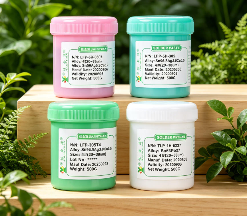
Solder paste and red glue processes can be mixed on the same PCB, but the physical isolation between the red glue dispensing position and the solder paste printing area must be strictly controlled, the reflow soldering temperature profile must take into account both the red glue curing and solder paste melting windows, and the stencil aperture design, dispensing parameters and AOI inspection strategy must be collaboratively optimized. Otherwise, it is extremely easy to cause batch defects such as cold solder joints, tombstoning or red glue contamination of pads. This is a high-risk but implementable special process combination in SMT processes.
Published: 2024-09-13SMT printing is a key process in which SMT stencils evenly transfer solder paste to PCB pads, directly affecting placement accuracy and reflow soldering yield. In actual production lines, solder paste viscosity, stencil aperture size, squeegee pressure, and printing speed must be coordinated and matched; any slight deviation will cause typical defects such as insufficient solder, solder bridging, or misalignment.
Published: 2024-07-28PCBA soldering materials have complete SGS certifications, covering all categories including lead-tin alloys, lead-free solder pastes, fluxes and cleaning agents, and comply with mandatory export standards such as IEC 61249, RoHS 2.0 and REACH. They can be directly used for complete machine exports to the EU, North America, Japan and South Korea, avoiding customs clearance delays or batch returns caused by missing material qualifications.
Published: 2024-07-14Solderability of immersion silver (ImAg) PCBs poses dual challenges to solder paste in terms of wetting performance and corrosion resistance. Jiajinyuan GJ-812A solder paste demonstrates excellent compatibility with silver finishes in actual production lines. Its weakly acidic flux system ensures sufficient wetting for 0.3mm fine-pitch QFN packages while avoiding excessive corrosion of the immersion silver layer. After reflow, the solder joints exhibit a clean surface and uniform IMC layer, effectively reducing the risks of cold solder joints and black pad.
Published: 2024-03-12For the typical solder paste defect of solder paste flux splatter contaminating PCBs, actionable improvement countermeasures that can be implemented immediately are proposed from four aspects: solder paste selection, stencil aperture design, printing parameter matching, and pre-reflow standing control. The synergistic matching of solder paste flux activity and viscosity is emphasized, avoiding reliance solely on cleaning or process compromises.
Published: 2024-01-16Soldering on ENIG boards imposes extremely stringent requirements on the halogen residue, wettability, and residue insulation of solder paste. Halogen-free solder paste stands out in preventing excessive dissolution of the gold layer, reducing leakage current during ICT testing, and improving long-term reliability. Jiajinyuan's halogen-free solder paste has been validated on multiple high-end HDI board production lines, demonstrating stable printability under 0.3mm pitch QFN and 0.4mm BGA packages, along with an actual void rate of <8%.
Published: 2023-07-11Our technical team is always ready to provide professional solder material selection advice and SMT process solutions.