SMT Solder Paste Manufacturers.

Focused on SMT soldering processes, a one-stop electronic soldering solutions provider.

Here you can find knowledge about PCB Wave Soldering Solder Bar, including but not limited to usage methods, installation techniques, troubleshooting and more. Focused on SMT soldering processes. If you can't find what you need, please contact us anytime.
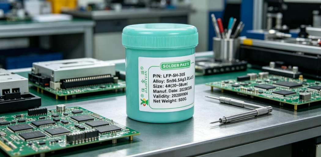
Choosing between solder paste and solder wire for mixed-technology PCB rework hinges on thermal profile control, joint geometry, flux activity, and residue management. Solder paste excels in QFN/DFN reballing and fine-pitch BGAs where precise volume control and uniform wetting—up to 100% with 8MQP/5RQ series—are critical, while solder wire remains practical for through-hole or large-pad hand-soldering at 240–260°C with Sn96.5Ag3Cu0.5 alloy. Key differentiators include paste viscosity stability over 8 hours, T4/T5 powder size distribution for stencil release, and halogen content under 500 ppm for high-reliability telecom or automotive applications.
Published: 2026-10-27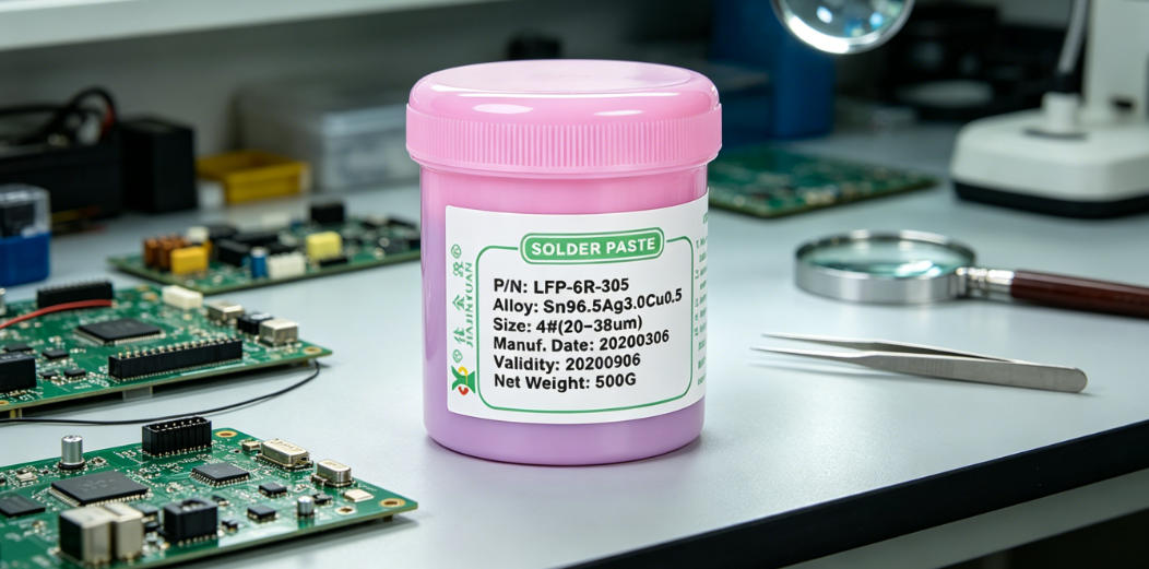
This article introduces a comprehensive portfolio of halogen-free, lead-free solder paste solutions engineered for consistent reliability across pure lead-free and mixed-technology PCB assemblies, covering high-temperature reflow, medium- and low-temperature applications, laser and iron-tip soldering, water-washable cleaning, and specialized stainless steel or aluminum joining; with verified alloy melting points from 65°C to 275°C, halogen content as low as 0 ppm, wetting performance up to 100% on QFN/DFN, and proven resistance to cold/hot slump under high humidity, these solder pastes deliver actionable process stability for SMT engineers managing complex thermal and material compatibility challenges.
Published: 2026-10-17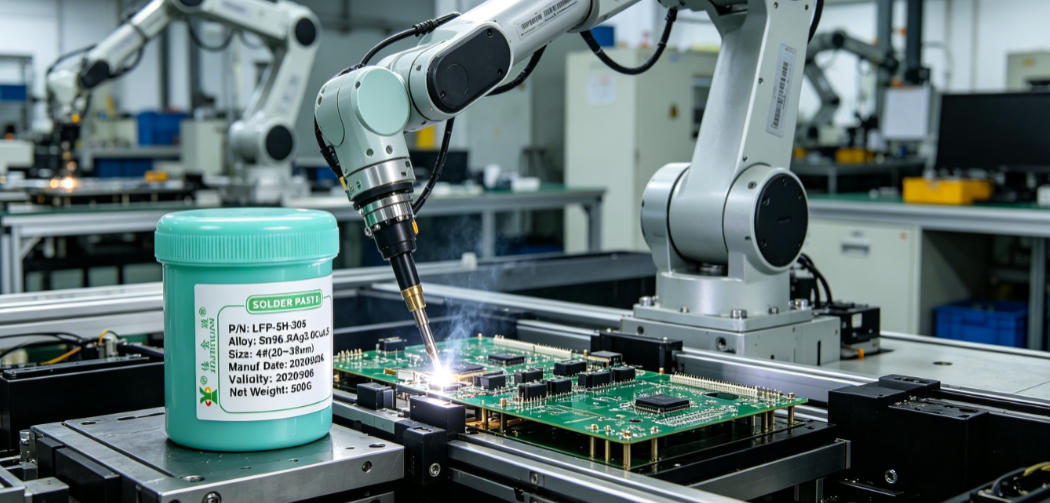
Reliable solder paste performance across lead free and mixed technology PCBs delivers consistent wetting, minimal voiding, and stable rheology under varying thermal and humidity conditions, with halogen-free and zero-halogen options supporting automotive, telecom, and consumer electronics; multiple alloy systems including 0307, 305, Sn64Bi35Ag1, and In52Sn48 enable precise thermal matching from 110°C to 260°C reflow, while T3–T7 powder distributions ensure high-resolution printing for QFN, DFN, and 01005 components without bridging or slump.
Published: 2026-10-16
The amount of PCBA solder paste directly affects soldering quality and production efficiency. Reasonably controlling the amount of solder paste can reduce waste and improve product reliability. In actual production, comprehensive adjustments need to be made in combination with factors such as stencil aperture design, printing parameters, and component layout to ensure that the solder paste evenly covers the pads and avoid problems such as cold solder joints or short circuits.
Published: 2026-08-28
Addressing the widespread issue of excessive solder paste voids in high-thermal-dissipation PCBs during SMT reflow soldering, this paper draws on 20 years of practical production line experience to systematically outline 6 types of high-frequency failure phenomena. These cover real-world causes including heat sink design defects, mismatched stencil apertures, improper solder paste selection, uncontrolled printing parameters, imbalanced reflow profiles, and fluctuating nitrogen purity. For each cause, immediately actionable calibration steps and routine preventive measures are provided, directly targeting the core process bottlenecks for SMT void improvement in high-thermal-dissipation PCBs.
Published: 2026-08-27
SMT soldering of thick copper boards is prone to cold solder joints and insufficient soldering due to their large heat capacity and delayed temperature rise. Solder paste activity matching and precise control of the reflow temperature profile are required to ensure solder joint reliability. The ramp-up rate in the preheating zone must be controlled between 0.5℃/s and 1.5℃/s, and the peak temperature must meet the component class limits specified in IPC-J-STD-020D. Otherwise, batch failures such as solder balls, tombstoning, and PCB delamination will occur.
Published: 2026-08-27
PCB pad plating directly affects solder paste wettability. Different plating types exhibit significant differences in interfacial reaction rate, intermetallic compound formation, and oxidation tendency during the reflow phase, leading to frequent defects such as cold solder joints, tombstoning, and poor solder wetting. Based on real production line failure cases, this article directly addresses the practical performance differences of mainstream plating types including ENIG, OSP, immersion silver, and HASL across solder paste printing, component placement, and reflow stages.
Published: 2026-08-27
Flux spatter from solder wire causing PCB component damage is a common persistent issue in SMT rework and hand soldering, rooted in differences in flux activity, volatilization rate, melt viscosity, and solder wire structure. Based on production line measurements, this paper compares the spatter tendency, residual corrosivity, and operational tolerance window of three types of solder wire flux—rosin-based, no-clean, and water-soluble—in typical scenarios such as 0402 chip resistor rework, QFN32 thermistor device touch-up soldering, and high-power LED pad reinforcement. It explicitly recommends rosin-based solder wire for high-density fine-pitch rework, restricts water-soluble type exclusively to copper-free bare aluminum substrates, and identifies no-clean type as having the best overall performance in conventional through-hole and double-sided board soldering.
Published: 2026-08-27
During the reflow soldering process of a moisture-absorbed PCB, internal water vaporizes rapidly, causing solder paste splattering. This is essentially caused by the conflict between MSL level failure as specified in J-STD-020D and the acceptability criteria in IPC-A-610G. When the PCB moisture absorption exceeds 0.15%wt and the heating rate in the preheat zone exceeds 3℃/s, the water vapor pressure exceeds the strength of the solder paste film layer, triggering splattering. Frontline operators often mistakenly attribute this to excessively high solder paste activity, while ignoring out-of-control baking parameters.
Published: 2026-08-27
Oxidation of PCB solder pads severely impairs the wettability of SMT soldering and the formation of intermetallic compounds. Even using high-activity solder paste and optimizing the reflow profile cannot compensate for the lack of interfacial bonding strength. The solderability of copper pad surfaces must be restored through source control, chemical activation, and coordinated process parameters.
Published: 2026-08-27Our technical team is always ready to provide professional solder material selection advice and SMT process solutions.