SMT Solder Paste Manufacturers.

Focused on SMT soldering processes, a one-stop electronic soldering solutions provider.

Here you can find knowledge about Wave Soldering Solder Bar, including but not limited to usage methods, installation techniques, troubleshooting and more. Focused on SMT soldering processes. If you can't find what you need, please contact us anytime.
The process parameter debugging of selective wave soldering should focus on the coordinated matching of nozzle temperature, chain speed, tin immersion time, and nitrogen coverage intensity. In actual production lines, Jiajinyuan equipment can significantly suppress bridging defects between pins of QFP-44 and SOIC-28 devices by controlling the nozzle temperature at 255℃±2℃, setting the chain speed at 0.8m/min, maintaining the single-point tin immersion time at 3.2 seconds, and stabilizing the nitrogen flow rate at 12L/min, which is especially suitable for secondary soldering scenarios after rework of high-density double-sided boards.
Published: 2013-01-16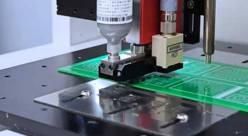
The purity of solder bars directly affects the quality of wave soldering joints. 99.99% purity solder bars can significantly reduce the rate of solder joint voids and poor wetting, while solder bars containing lead or excessive impurities are prone to forming solder balls, sharp protrusions, and bridging defects at the edges of PCB pads. Production line measurements show that for every 0.005% excess in the total amount of impurities such as copper, iron, and arsenic in the solder bars, the rate of cold solder joints increases by 12% to 18%.
Published: 2012-11-17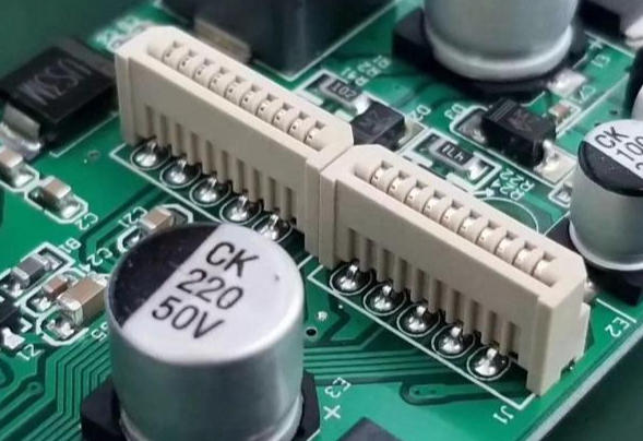
The frequency of adding wave soldering bars depends on the average daily soldering volume, temperature fluctuation of the solder pot, and the accumulation rate of impurities. Typically, additional solder bars need to be replenished every 8 to 12 hours. During replenishment, it is necessary to simultaneously clean the dross, calibrate the liquid level, and ensure that the new solder bars are preheated to above 180°C before being slowly immersed, so as to avoid unstable solder waves or aggravated oxidation caused by cold material impact.
Published: 2011-12-24Dip soldering is a core process for high-volume PCBA pin soldering. The composition, melting point, and oxidation control of wave soldering solder bars directly determine solder joint wettability and cold solder joint rate. Jia Jinyuan wave soldering solder bars can maintain a solder wave height deviation of ≤0.3 mm and a solder dross generation rate of less than 1.2% during 8 consecutive hours of production, significantly reducing fixture rework frequency.
Published: 2011-07-29Jia Jinyuan provides free solder sample testing and sample mailing services. All solder sample tests are conducted synchronously on real SMT placement lines and wave soldering production lines, covering mainstream packages such as 0201 to QFN48. The measured yield data can be traced back to the furnace temperature curve and AOI original image of each batch. The solder sample test results are directly related to the customer's existing stencil opening, reflow soldering temperature setting and flux compatibility.
Published: 2011-06-14Circuit board soldering covers core processes such as SMT placement, wave soldering, and manual soldering, each of which imposes stringent requirements on solder paste printing accuracy, temperature profile control, flux selection, and PCB board deformation tolerance. Production line tests by Jia Jinyuan show that for 0.3mm pitch QFN devices, a reflow soldering peak temperature deviation exceeding ±2℃ causes cold solder joints, while insufficient wave soldering fixture press-in depth below 0.15mm leads to through-hole solder joint climb height falling below the 0.75mm standard value.
Published: 2011-05-22Domestic solder covers wire diameters from 0.3mm to 3.0mm, all temperature ranges (183℃~227℃) for both leaded and lead-free variants, and three flux systems: rosin, no-clean, and water-washable. It is compatible with multiple scenarios including high-speed SMT printing, wave soldering, dip soldering, and manual touch-up soldering. The Jiajinyuan series has a measured wetting angle ≤35°, bridging rate below 0.08%, and residual ion content <0.5μg/cm2. No adjustment to stencil apertures or reflow temperature profile is required when switching materials on the production line.
Published: 2011-03-06Addressing the local soldering challenges of industrial control board connectors, selective wave soldering achieves high-reliability soldering through precise temperature control and solder wave positioning, while avoiding overheating damage to sensitive components across the entire board. Jiajinyuan equipment stably achieves a 99.7% first-pass yield under conditions of 0.8mm pin pitch and 12mm pad length, with a process window widened by 35% compared to traditional wave soldering, making it particularly suitable for the mixed assembly requirements of multilayer boards + high-density connectors in domestic substitution.
Published: 2010-08-27
High impurity content in solder bars directly causes typical wave soldering defects such as solder spikes, bridging, and cold soldering. Elements such as copper, iron, and arsenic in solder impurities not only reduce wettability, but also accelerate oxidation of the solder pot and clog the nozzles, seriously affecting the line throughput yield and the service life of the solder bars.
Published: 2010-08-24Solder used in electronics manufacturing plants must achieve dynamic matching across all processes including SMT placement, wave soldering, and touch-up soldering. Jiajinyuan solder adapts to complex thermal stress scenarios with reflow peak temperature of 235℃, wave soldering temperature of 260℃, and manual touch-up soldering instantaneous temperature of 380℃ through melting point gradient design. Its active residue content is controlled within 0.012%, avoiding ICT test leakage and excessive ion contamination.
Published: 2010-03-28Our technical team is always ready to provide professional solder material selection advice and SMT process solutions.