SMT Solder Paste Manufacturers.

Focused on SMT soldering processes, a one-stop electronic soldering solutions provider.

Here you can find knowledge about BGA Solder Paste, including but not limited to usage methods, installation techniques, troubleshooting and more. Focused on SMT soldering processes. If you can't find what you need, please contact us anytime.
X-Ray inspection can penetrate PCBs and packages to directly observe void ratios, bridging, cold solder joints, and offset conditions at the bottom of devices such as BGAs and QFNs, avoiding missed judgments in blind spots that cannot be covered by traditional AOI and ICT. It is the most reliable non-destructive method for verifying reflow soldering quality in SMT processes.
Published: 2022-03-16When SMT mounting 01005 and BGA precision components, extremely high placement accuracy is required. It is necessary to simultaneously control the nozzle vacuum stability, visual system calibration error, PCB thermal deformation, and solder paste collapse state. Any slight deviation will cause batch defects such as tombstoning, cold solder joints, and solder bridges. Actual measurements on the Jiajinyuan production line show that a placement offset exceeding 25 μm for 01005 devices leads to a 37% increase in open circuit rate after reflow. Poor coplanarity of BGA solder balls is directly related to placement pressure fluctuations exceeding 0.3 N.
Published: 2022-01-28BGA voiding is a typical SMT defect that directly affects device heat conduction and solder joint reliability. Production line data from Jiajinyuan shows that a void rate exceeding 25% triggers batch rework. Based on real retrospective cases, this paper conducts a two-way investigation from four key dimensions: solder paste activity degradation, deviations in stencil aperture design, peak temperature fluctuations in the reflow profile, and insufficient nitrogen purity, clarifying the coupling relationship between material batch anomalies and printing parameter drift.
Published: 2021-11-03
For BGA high-density packaging scenarios, Jiajinyuan's halogen-free, low-void solder paste 8M9P/5RR series has completed production line verification at leading packaging and testing customers. The measured void rate is stably controlled within 3%. After reflow soldering, the solder joints exhibit uniform wetting and a dense, continuous IMC layer, raising the first-pass yield of BGA devices from 92.7%
Published: 2021-07-14When reflow soldering precision BGA/QFN devices, the heating rate directly affects solder joint void ratio, solder ball collapse consistency, and PCB warpage risk. In particular, a preheat ramp exceeding 3℃/s can easily cause ceramic substrate cracking, while insufficient flux residue control occurs when the soak stage duration below 150℃ is less than 90 seconds. Jia Jinyuan's measured data shows that the void ratio of QFN bottom solder joints increases by 27% as the heating slope rises by 1.2℃/s. The temperature difference across the entire board must be controlled within ±2.5℃ to ensure first-pass yield.
Published: 2021-03-25When soldering BGA devices on thick copper boards, due to the large heat capacity and slow heating rate, the flux in the solder paste does not volatilize sufficiently and gas escape is hindered, making it extremely easy to form void defects inside solder joints. It is necessary to select a special solder paste with low residue, high activity, and a wide reflow window; otherwise, the void rate generally exceeds 25%, far exceeding the requirement of ≤15% for IPC-A-610 Class G.
Published: 2020-12-08BGA soldering in 5G communication and energy storage motherboards faces challenges of high thermal stress, long-term aging, and high-frequency signal integrity. By optimizing stencil aperture design, segmented temperature control of reflow profile, and post-soldering full X-ray inspection process, JJY ensures that BGA solder joints have no void expansion and no abnormal IMC thickening after 1000 hours of accelerated aging at 85℃/85%RH, achieving true long-term reliability.
Published: 2020-08-15The head-in-pillow effect caused by solder paste defects and X-ray void defects in BGA soldering require coordinated troubleshooting from four aspects: solder paste selection, stencil design, printing parameters, and reflow profile. Insufficient wetting, uneven flux volatilization, or pad oxidation during the solder paste soldering process will exacerbate solder paste defect manifestations. Combining X-Ray image features can quickly identify the root cause of voids.
Published: 2019-12-14When soldering thick copper PCBs and multilayer boards with BGA, the significantly increased thermal capacity means conventional heating parameters can easily cause cold solder joints or chip warpage. It is necessary to specifically extend the preheating time, increase the temperature of the soaking zone, and slow down the peak heating slope to ensure synchronous melting of solder balls and overall thermal balance of the PCB.
Published: 2019-04-12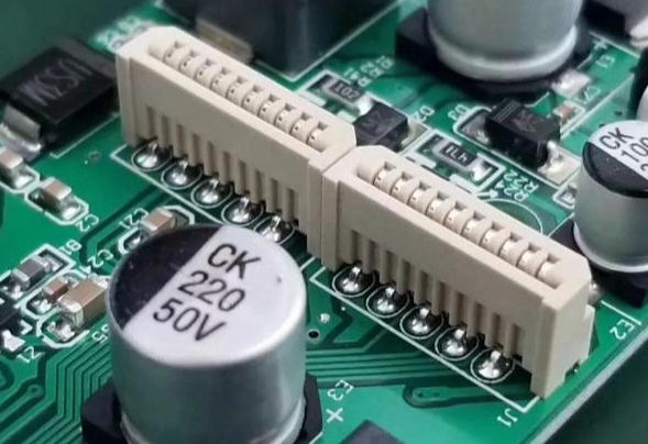
What solder paste to use for BGA repair and how to select the appropriate activity level directly affects the first-pass rework success rate and solder joint reliability. Production line verification by JJY shows that medium-activity RMA solder paste balances wettability and controllable residue in most BGA soldering scenarios; high-activity RA solder paste is only suitable for special chips with severe oxidation or poor plating, while no-clean solder paste must be paired with nitrogen-protected reflow conditions.
Published: 2018-06-29Our technical team is always ready to provide professional solder material selection advice and SMT process solutions.