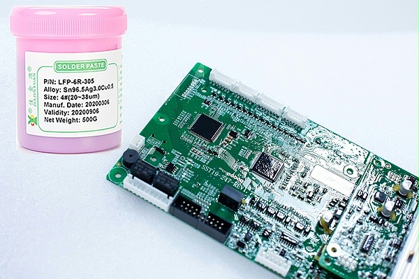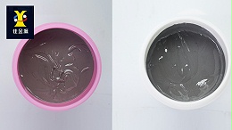
SMTPrinting technology andPCBThe quality of the circuit board scheme has an impactSMTLead-free solder pasteThe printing effect.PCBThe circuit board solution is excellent and can prevent poor printing phenomena such as component offset and suspension Bridges. Today, JJY lead-free solder Paste Manufacturer will talk about the benefitsSMTPrinted with lead-free solder pastePCBKnowledge of process requirements:

SMTPrinted with lead-free solder pastePCBProcess requirements:
1Theoretically, the amount of printed solder paste per unit area of the pad is usually:
①For general components, it is0.8mg/mm2Left and right.
②For fine-pitch devices, it is0.5mg/mm2Left and right.
2The solder paste is printed evenly;The thickness range of solder paste isMASKThe thickness of the template-15%~+20%:
MASKThe optimal thickness specifications for template thickness and printing thickness range
MASKTemplate thickness Printing thickness range Typical values of printing thickness
0.18mm 0.15~0.22mm 0.20mm
0.15mm 0.13~0.18mm 0.16mm
0.13mm 0.11~0.16mm 0.14mm
0.10mm 0.08~0.13mm 0.11mm
3The area covered by the printed solder paste on the solder pad should be80%That's all.
4The demolding and forming of the printed solder paste are excellent;There should be no collapse or fracture,No wire connection offset, neat edges, etc.
①For general components(Such as0603Or above specifications)Offset out of the pad no more than0.2mm;
②For fine-pitch devices(Such asPITCH≤0.5mmIC)Offset out of the pad no more than0.1mm;
③For0402Or the following specificationsCHIPThe offset of the chip component from the pad is no more than0.1mm;
5Ensure the cleanliness of the substrate and solder paste, substrate(Such as the gold finger area)It is not allowed to be contaminated by solder paste.
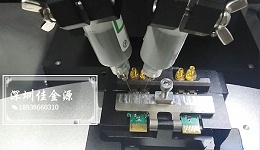
Solder paste printing
The following is lead-free solder paste during printingPCBThe basic elements of the circuit board scheme:
1At both endsPCBThe circuit board must be symmetrical, which can ensure the balance of the surface tension of lead-free solder paste when it drops during printing, making the solder joints precise and error-free.
2,PCBThe pad spacing of the circuit board should be well controlled. The printing of lead-free solder paste also depends on the consistency between the pad spacing and the distance between the pins of electronic components. Both too large and too small spacing will have an impact on the printing of lead-free solder paste.
3,PCBThe remaining dimensions of the circuit board should be well controlled. The solder joints formed after the electronic components are connected to the solder pads must be ensured to be able toPCBA crescent surface is formed on the solder pad to ensure that the solder joints of the lead-free solder paste are smooth and full.
4,PCBThe width of the solder pads must be consistent with that of the electronic components; otherwise, lead-free solder paste will also produce soldering defects during printing.
5The through hole must not be placed on the pad. If the through hole is on the pad, it will cause the solder of the lead-free solder paste to flow out from the through hole during printing, resulting in insufficient solder for the lead-free solder paste and affecting the soldering quality.
The above is about benefitsSMTPrinted with lead-free solder pastePCBKnowledge of process requirements, I hope it will be helpful to everyone! If you want to learn more about solder paste, please keep following JJY lead-free solder Paste Manufacturer and leave a message online to interact with us.


