pcbaIn the processing technologySolder pasteAnalysis of Printing Issues? This printing process is still of great significance after all. Solder paste printing is very complicated and has a very important impact on the quality of the product in the later stage. Therefore, many problems arise at this time regarding the quality of the product, which directly determines itPCBAWhether the production is good or bad, so in this process, everyone should pay more attention to some issues and analyses. Now, let's have JJY solder Paste Manufacturer explain:
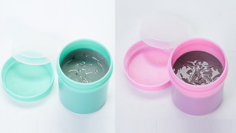
④Solder paste sharpening can easily cause a short circuit after soldering.
SMTSolder paste printing steps
1Pre-printing inspection
ACheck what is to be printedPCBThe correctness of the board
BCheck what is to be printedPCBWhether the surface of the board is intact, free of defects and dirt;
CCheck whether the steel mesh is compatible withPCBConsistency, and whether its tension meets the printing requirements;
DCheck whether there are any blocked holes in the steel mesh,If there is a clogging phenomenon, the steel mesh should be wiped with lint-free paper dipped in alcohol,And dry it with an air gun,The air gun should be kept in contact with the steel mesh when in use3-5CMThe distance
ECheck whether the solder paste used is correct and whether it is used in accordance with "Storage and Use of Solder Paste". Note: Pay attention to the warming time, stirring time, and the distinction between lead-free and leaded, etc.
Ii.SMTSolder paste printing
1Fix the correct steel mesh onto the printing machine and debug itOK;
2Assemble the clean and good scraper onto the printing press;
3Use a solder paste mixer to add the solder paste to the steel mesh. The first time you add the solder paste, the height should be1CMLeft and right, width1.5-2CMLength viewPCBThe length is determined, with both sides longer than the printed area3CMLeft or right is fine. It should not be too long or too short. Add the solder paste every two hours thereafter, with an amount of approximately100G;
4Put inPCBPlate printing, before printing5PCSThe board is required to undergo a full inspection to ensure the printing qualityOKAfterwards, notifyIPQCAfter conducting the first inspection and confirming that there are no abnormalities in the printing quality, notify the production line operators to start production.
5During the normal printing process, the operator needs to check the printing effect every half an hour to see if there are any defects such as insufficient solder, continuous solder, sharp edges, displacement, or missed printing. For components with overly dense pins, such asBGA,QFP,SOPFocus on checking the printing effect such as "power strips", etc.
6Every printing5PCSThe steel mesh needs to be cleaned once, ifPCBThere are components with overly dense pins on the board.BGA,QFP,SOPFor power strips, the cleaning frequency should be increased every time3PCSClean once;
7During the production process, if it is found to be continuous3PCSIf the printing is poor, notify the technician for debugging. Clean the poorly printed onesPCBBoard. Poor cleaning and printingPCBWhen scraping, do not use hard objects directlyPCBThe surface layer is protected from scratchesPCBThe surface line has gold fingersPCBAvoid gold fingers. Wipe repeatedly with lint-free paper mixed with a little alcohol, then dry with an air gun. Check under a magnifying glass. If there is no residual solder paste, it is considered goodOK;
8During the normal printing process, it is necessary to regularly check whether the solder paste is overflowing and collect the spilled solder paste.
9After production is completed, solder paste, scrapers, steel mesh and other auxiliary materials and tools should be recovered, and the tooling fixtures should be cleaned. The specific operations should be carried out in accordance with the "Storage and Use of Solder Paste" and the "Steel Mesh Cleaning Operation Guidelines".
Iii. Requirements for Solder Paste Printing Process
The main printing defects are: insufficient solder, continuous solder, sharpening, displacement, missed printing, excessive solder, and collapse.PCBThe plate is dirty, etc. The thickness of the solder paste printing is the thickness of the steel mesh-0.02mm~+0.04mm; Ensure that the welding effect after the furnace is defect-free;
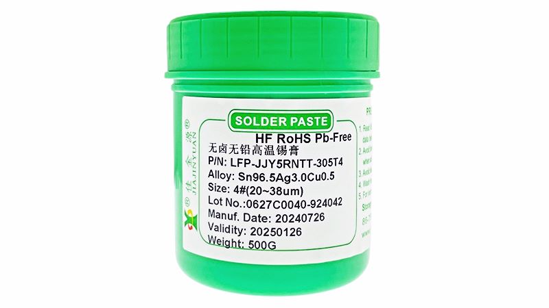
Alright, these are some of the issues related to process printing that we have introduced. You can go and take a look. This will help you do a better job in your subsequent operations. If you still have any questions, you are welcome to consult Shenzhen JJY Industrial Technology Co., LTD. Let's learn and grow together! Solder wire of JJY brandSolder pasteSolder rods, always looking forward to your companions coming to take them away together.
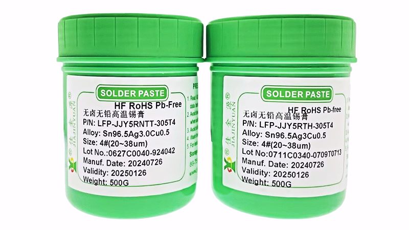
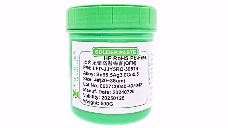

 Tel:+86 0755 88366766
 Phone:+86 18938660310
 Email:sales@jjyhanxi.com
 Address:13/F,12/F, Building No. B,Qinghu Technology Park,Qingxiang Rd.,Qinghu Community, Longhua Subdistrict,Longhua District,Shenzhen City,GUANGDONG Province,P.R.C.(518027)
 Guangdong Public Security Backup 44030902002666 name
 WeChat
 WeChat official account
