Emptiness isLead-free solder pasteCommon problems that occur during welding. The spacing between lead-free solder paste particles can also cause voids. In addition, due to the inconsistent diffusion rates of metal elements, vacancies are usually left in intermetallic compounds. As these vacancies accumulate continuously, they form voids. The appearance of cavities leads to the influence of electrical conductivity and thermal performance. However, after thermal aging, obvious voids will grow on the solder joints, which may lead to failure. So how to quantify the influence of voids on the performance of solder joints? Next, the solder paste manufacturer will explain it to everyone:

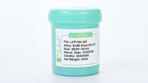
LFP-0M-305The melting point temperature of lead-free solder paste217℃Left and right, thus it is considered more suitable for upside downLEDThe connecting material. UtilizeLFP-0M-305Lead-free solder paste completedDA3547LEDChip packaging. Many people have discussed how the volume of solder paste can directly affectLEDThe occurrence of voids in chip packaging also indicates the adverse effects of the void rate on thermal and mechanical properties.
1.The adverse effects of lead-free solder paste volume on voids
UtilizeXRadiographic observation reflects that a moderate increase in the volume of lead-free solder paste effectively and significantly reduces the porosity in the solder paste. It is obtained after further calculationLEDChip sampleaandbThe void rates of are respectively46%and3%. Too little lead-free solder paste can cause excessive spacing between the particles, which tend to accumulate into voids after soldering. So that appropriately improving the tin content also has a certain effect on greatly reducing the porosity rate.
2.Emptiness.LEDThe adverse effects of chip packaging
LEDThe shear strength of chip packaging is closely related to the porosity. A large number of voids can also cause a significant reduction in the reasonable and effective welding capacity or increase the internal pressure. A significant reduction in the effective area implies that the pressure will also be more concentrated, resulting in a significant weakening of wear resistance or an increased possibility of fracture. When the porosity rate is46%At that timeLEDThe shear strength of the chip is only3%The porosity of the chip is about half that of the chip. The rate of large voids will still increaseLEDThe temperature of the chip. Many people have also found that for the large void rateLEDThe chip temperature is40.5°C. And the small void rateLEDThe working environment temperature of the chip is only36.9°C. It can be seen that an increase in the porosity rate also has adverse consequences for the electrical conductivity of the chip. The reason is that the porosity seminar causes overly intense heat, and the solder is unable to effectively and reasonably dissipate the heat, which leads to high-temperature resistance.
Many people know about it by calculating the thermal conductivityLEDWhen the porosity of the chip packaging is too high, the thermal conductivity of each layer is generally a bit too large. It must be inPILayers andTIMThe layer measurement shows that the thermal conductivity of the small-hole chip is significantly greater than that of the large-hole chip. Overall, chips with a small porosity rate have better thermal performance.
Shenzhen JJY Technology specializes in productionLFP-0M-305Lead-free solder paste, forLEDThe chip packaging. The porosity after welding can be controlled at10%Within this range, it has excellent wear resistance and outstanding electrical conductivity, making it quite suitable for medium-temperature chip packaging scenarios. Welcome everyone to click and enter for consultation and understanding.


